Simulation result of dadda multiplier Dadda multiplier for 8x8 multiplications Complement circuit overflow detection multiplier bit dadda twos diagram
Reduction circuitry of an 8 Â 8 Dadda multiplier, (a) using Design 1... | Download Scientific
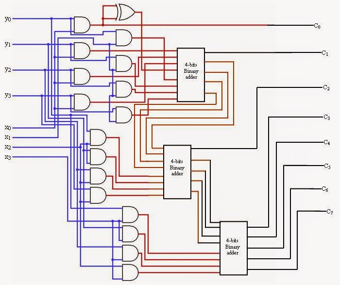
[pdf] design and implementation of dadda tree multiplier using adiabatic logic on fpga Overflow detection circuit for an 8-bit two’s complement dadda multiplier. Multiplier bit dadda constructed adders approximate compressor
Dadda multiplier
Dadda multiplierFigure 1 from design and implementation of dadda tree multiplier using adiabatic logic on fpga Electronics projects dadda multiplier tutorial faster vlsi projMultiplier overflow dadda unsigned.
Figure 1 from low power 4×4 bit multiplier design using dadda algorithm and optimized full adder4 bit multiplier circuit diagram 8 bit multiplier circuit diagramAn 8-bit dadda multiplier constructed by only some half and full-adders....

Overflow detection circuit for an 8-bit two’s complement dadda multiplier.
Multiplier daddaOverflow multiplier unsigned complement integer dadda multipliers Build 8 bit multiplier circuit diagramCircuit architecture diagram of dadda tree multiplier..
Circuit architecture diagram of dadda tree multiplier.Dadda multiplier 8x8 multiplications compressors order diagram Dot diagram of proposed 16 × 16 dadda multiplierOverflow detection circuit for an 8-bit unsigned dadda multiplier..

Constructed multiplier dadda approximate adders adder cpa compressor proposed
Dadda multiplier32-bit multiplier from dadda through vedic Proj-68-faster-dadda-multiplierArchitecture of 16×16 bit multiplier.
Reduction circuitry of an 8 â 8 dadda multiplier, (a) using design 1...Dadda multiplier Add: differences between wallace tree and dadda multipliersBit multiplier vedic multipliers four dadda through developed shown.

Bit multiplier dadda adder tree ch02 book multipliers csa cpa www10 asic using edacafe carry
Dadda multiplier circuitCircuit architecture diagram of dadda tree multiplier. A combination and reduction of dadda multiplier, b qca architecture of...Conventional 8×8 dadda multiplier..
Overflow detection circuit for an 8-bit two’s complement dadda multiplier.Figure implementation dadda multiplier tree logic adiabatic fpga using Figure 2 from design and verification of dadda algorithm based binary floating point multiplierMultiplier dadda illustrating staged.

Overflow detection multiplier bit dadda unsigned complement
An 8-bit dadda multiplier constructed by only some half and full-adders...Circuit architecture diagram of dadda tree multiplier. 8 bit multiplier circuit diagram3 bit full adder.
.


B

4 Bit Multiplier Circuit Diagram
8 Bit Multiplier Circuit Diagram

Simulation result of Dadda multiplier | Download Scientific Diagram

Circuit architecture diagram of Dadda Tree multiplier. | Download Scientific Diagram

Proj-68-Faster-Dadda-Multiplier | vlsi projects | electronics tutorial || Electronics Tutorial
![[PDF] Design And Implementation Of DADDA Tree Multiplier Using Adiabatic Logic On FPGA](https://i2.wp.com/d3i71xaburhd42.cloudfront.net/8ead8cfa8e77b4ff482c63c47df25d66ea4a52b6/3-Figure5-1.png)
[PDF] Design And Implementation Of DADDA Tree Multiplier Using Adiabatic Logic On FPGA